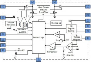
Diodes is aiming at phones, tablets, and other battery-operated consumer devices with a synchronous buck/boost dc-dc converter with integrated high-side and low-side 25mΩ H-bridge mosfets.

Called AP72200, it delivers up to 97% efficiency with 1% voltage regulation accuracy, low quiescent current, and very low output ripple.
Using proprietary buck/boost current-mode control, it can handle continuous current up to 2A and work over 2.3 – 5.5V on its input to produce 2.6 – 5.14V (in 0.02V increments is over I2C, see below).
Many of its features are user-configurable through an I2C interface, which can operate in standard mode, fast mode, fast-mode plus, and high-speed mode.
Features include output disable, programmable-output voltage ramp-up and ramp-down slew-rates, output-active discharge, over-voltage protection threshold, and over-current threshold.
The chip can also be configured to operate in PWM or PFM mode, as well as in ultrasonic mode, which reduces the switching frequency to avoid the generation of sub-harmonic frequencies in the region of 20kHz that can cause interference in the audible frequency range.
Mosfet shutdown current is less than 1µ and chip quiescent current can be as low as 20µA when operating in non-switching mode, and typically 29µA in PFM mode.
Continuous-mode switching frequency is typically 2.5MHz, dropping to 27kHz in ultrasonic mode.
It comes in a 2.125 x 1.75mm 20 ball WLCSP package.
Source from:electronicsweekly

 Englisch
  Chinesisch
  Deutsch
  Koreanisch
  Japanisch
  Farsi
Farsi  Portuguese
  Russian
  Spanisch


